Here we are providing Class 12 Physics Important Extra Questions and Answers Chapter 14 Semiconductor Electronics: Materials, Devices and Simple Circuits. Important Questions for Class 12 Physics with Answers are the best resource for students which helps in Class 12 board exams.
Class 12 Physics Chapter 14 Important Extra Questions Semiconductor Electronics: Materials, Devices and Simple Circuits
Semiconductor Electronics Important Extra Questions Very Short Answer Type
Question 1.
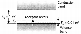
Draw the energy band diagram for a p-type semiconductor.
Answer:
The energy level diagram is shown below.
Question 2.
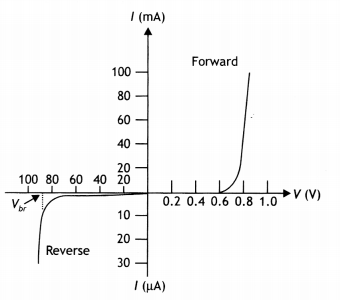
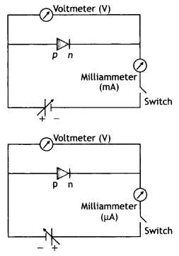
Draw the voltage-current characteristic of a p-n junction diode in forwarding bias and reverse bias.
Answer:
The characteristics are as shown.
Question 3.
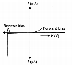
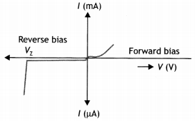
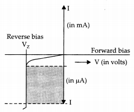
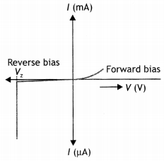
Draw the voltage-current characteristic for a Zener diode.
Answer:
The V-l characteristic of the Zener diode is as shown.
Question 4.
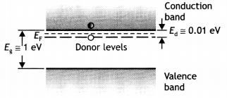
Draw the energy band diagram for n-type semiconductor.
Answer:
The diagram is as shown.
Question 5.
An ac input signal of frequency 60 Hz is rectified by an
(i) Half wave and an
Answer:
The output frequency remains the same in a half-wave rectifier, i.e. 60 Hz.
(ii) Full-wave rectifier. Write the output frequency in each case.
Answer:
The output frequency becomes twice the input frequency in the case of the full-wave rectifier, i.e. 120 Hz.
Question 6.
Give the ratio of the number of holes and the number of conduction electrons in an intrinsic semiconductor.
Answer:
The ratio is one.
Question 7.
What is the depletion region in a p-n junction?
Answer:
It is a thin layer between p and n sections of the p-n junction which is devoid of free electrons and holes.
Question 8.
Name an impurity which when added to pure silicon makes it a
(i) p-type semiconductor
Answer:
Boron, aluminum, etc.
(ii) n-type semiconductor.
Answer:
Phosphorous, antimony, etc.
Question 9.
Which type of biasing gives a semiconductor diode very high resistance?
Answer:
Reverse biasing.
Question 10.
Identify the biasing in the figure given below.
Answer:
Forward biasing.
Question 11.
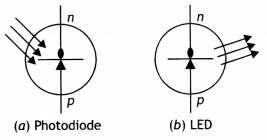
Draw the circuit symbol of (a) photodiode, and (b) light-emitting diode.
Answer:
The circuit symbols are as shown below.
Question 12.
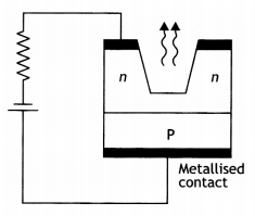
What is the function of a photodiode? (CBSE AI 2013C)
Answer:
It functions as a detector of optical signals.
Question 13.
When a p-n junction diode is forward biased, how will its barrier potential be affected? (CBSEAI 2019)
Answer:
Potential barrier decreases in forwarding bias.
Question 14.
Name the junction diode whose l-V characteristics are drawn below: (CBSE Delhi 2017)
Answer:
Solar cell.
Question 15.
How does the width of the depletion region of a p-n junction vary if the reverse bias applied to it decreases?
Answer:
With the increase in the reverse bias, the depletion layer increases.
Question 16.
How does the width of the depletion region of a p-n junction vary if the reverse bias applied to it decreases?
Answer:
If the reverse bias decreases, the width of the depletion layer also decreases.
Question 17.
Why is the conductivity of n-type semiconductors greater than that of p-type semiconductors even when both of these have the same level of doping?
Answer:
It is because in n-type the majority carriers are electrons, whereas in p-type they are holes. Electrons have greater mobility than holes.
Question 18.
How does the conductance of a semiconducting material change with rising in temperature?
Answer:
Increases with an increase in temperature.
Question 19.
How is a sample of an n-type semiconductor electrically neutral though it has an excess of negative charge carriers?
Answer:
It is because it contains an equal number of electrons and protons and is made by doping with a neutral impurity.
Question 20.
How is the bandgap, Eg, of a photodiode related to the maximum wavelength, λm, that can be detected by it?
Answer:
Eg = \(\frac{h c}{\lambda_{m}}\)
Question 21.
Zener diodes have higher dopant densities as compared to ordinary p-n junction diodes. How does it affect the
(i) Width of the depletion layer
Answer:
Junction width will be small and
(ii) Junction field?
Answer:
The junction field will be high.
Question 22.
Can the potential barrier across a p-n junction be measured by simply connecting a voltmeter across the junction? (NCERT Exemplar)
Answer:
No, because the voltmeter must have a resistance very high compared to the junction resistance, the latter being nearly infinite.
Semiconductor Electronics Important Extra Questions Short Answer Type
Question 1.
Draw a labeled circuit diagram of a full-wave rectifier using a p-n junction.
Answer:
The diagram is as shown.
Question 2.
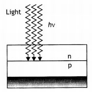
What is a solar cell? How does it work? Give one of its uses.
Answer:
It is a p-n junction used to convert light into electrical energy. In such a diode, one region either the p-type or the n-type is made so thin that light falling on the diode is not absorbed appreciably before reaching the junction. The thin region in the solar cell is called the emitter and the other is called the base. The magnitude of current depends upon the intensity of light reaching the junction. A solar cell can be used to charge storage batteries during the daytime, which can be used during the night.
These are used as power supplies for satellites and space vehicles.
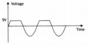
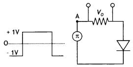
Question 3.
Draw the output signal in a p-n junction diode when a square input signal of 10 V as shown in the figure is applied across it. (CBSE AI 2019)
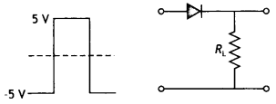
Answer:
The diode will conduct only when it is forward biased. Therefore, till the input voltage is + 5 V, we will get an output across R, accordingly the output waveform shown in the figure.
Question 4.
The following diagrams, indicate which of the diodes are forward biased and which are reverse biased.
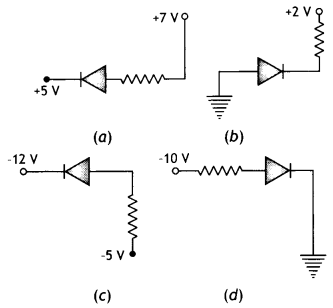
Answer:
(a) Forward biased.
(b) Reverse biased.
(c) Forward biased,
(d) Reverse biased.
Question 5.
Mention the important considerations required while fabricating a p-n junction diode to be used as Light-Emitting Diode (LED). What should be the order of bandgap of an LED if it is required to emit light in the visible range? (CBSE Delhi 2013)
Answer:
The important considerations are
- It should be heavily doped.
- The diode should be encapsulated with a transparent cover so that emitted light can come out.
The semiconductor used for the fabrication of visible LEDs must at least have a bandgap of 1.8 eV.
Question 6.
In the given circuit diagram shown below, two p-n junction diodes D1 and D2 are connected with a resistance R and a dc battery E as shown. Redraw the diagram and indicate the direction of flow of appreciable current in the circuit. Justify your answer.
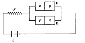
Answer:
The redrawn diagram showing the flow of appreciable current is shown below.
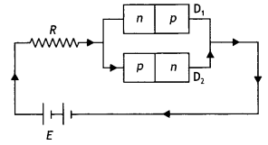
Here diode D2 is forward biased, hence it conducts. Therefore appreciable current will pass through it. However, diode 0, is reverse biased, hence negligible current will flow through it.
Question 7.
The diagram below shows a piece of pure semiconductor S in series with a variable resistor R and a source of constant voltage V. Would you increase or decrease the value of R to keep the reading of ammeter (A) constant when semiconductor S is heated? Give reason.
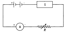
Answer:
When a semiconductor is heated, its resistance decreases. As a result, the total resistance of the circuit will decrease. In order to maintain constant current flow, the total resistance of the circuit must remain constant. Hence, the external resistance has to be increased to compensate for the decrease of resistance of the semiconductor.
Question 8.
Two semiconductor materials X and Y showed in the figure are made by doping germanium crystal with indium and arsenic respectively. The two are joined end to end and connected to a battery as shown,
(i) Will the junction be forward or reverse biased?
(ii) Sketch a V-l graph for this arrangement.
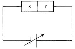
Answer:
Material X is p-type and material Y is n-type.
(i) The junction is reverse biased.
(ii) For the V-l graph
The characteristics are as shown.
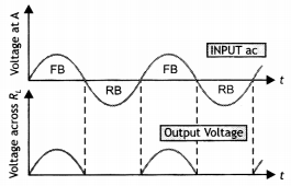
Question 9.
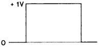
Draw the output waveform across the resistor (figure). (NCERT)
Answer:
It is a half-wave rectifier, therefore only the positive cycle will be rectified. Thus the output waveform is as shown.
Question 10.
(i) Name the type of a diode whose characteristics are shown in figure
(a) and figure (b).
(ii) What does point P in figure (a) represent?
(iii) What do the points P and Q in figure (b) represent? (NCERT Exemplar)
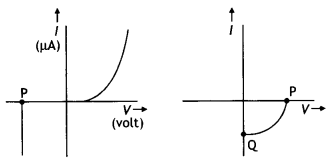
Answer:
(i) Zener junction diode and solar cell.
(ii) Zener breakdown voltage
(iii) P-open circuit voltage.
Q-short circuit current
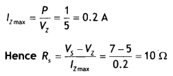
Question 11.
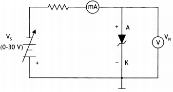
A Zener of power rating 1 W is to be used as a voltage regulator. If Zener has a breakdown of 5 V and it has to regulate voltage which fluctuated between 3 V and 7 V, what should be the value of R, for safe operation (figure)? (NCERT Exemplar)
Answer:
Given P = 1 W, Vz = 5V, Vs = 7 V, Rs = ?
We know that
Question 12.
Two material bars A and B of the equal area of the cross-section are connected in series to a dc supply. A is made of usual resistance wire and B of an n-type semiconductor.
(i) In which bar is the drift speed of free electrons greater?
(ii) If the same constant current continues to flow for a long time, how will the voltage drop across A and B be affected? Justify each answer. (CBSE Sample Paper 2018-19)
Answer:
(i) Drift speed in B (n-type semiconductor) is higher.
Reason: Since the two bars A and B are connected in series, the current through each is the same.
Now l = neAvd
Or
vd = \(\frac{1}{n e A}\) ⇒ vd ∝ \(\frac{1}{n}\) (As l and A are same).
As n is much lower in semiconductors, drift velocity will be more.
Question 13.
Explain how the width of the depletion layer in a p-n junction diode changes when the junction is (i) forward biased and (ii) reverse biased. (CBSE Delhi 2018C)
Answer:
The width of the depletion region in a p-n junction diode decreases when it is forward biased because the majority of charge carriers flow towards the junction. While it increases when the junction diode is reverse biased because the majority of charge carriers move away from the junction.
Semiconductor Electronics Important Extra Questions Long Answer Type
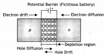
Question 1.
Define the terms ‘potential barrier’ and ‘depletion region’ for a p – n junction diode. State how the thickness of the depletion region will change when the p-n junction diode is (i) forward biased and (ii) reverse biased.
Answer:
Potential barrier: The potential barrier is the fictitious battery, which seems to be connected across the p-n junction with its positive terminal in the n-region and the negative terminal in the p-region.
Depletion region: The region around the junction, which is devoid of any mobile charge carriers, is called the depletion layer or region.
- When the p-n junction is forward biased, there is a decrease in the depletion region.
- When the p-n junction is reverse biased, there is an increase in the depletion region.
Question 2.
Explain (i) forward biasing and (ii) reverse biasing of a p-n junction diode.
Answer:
(i) A p-n junction is said to be forward-biased if its p-type is connected to the positive terminal and its n-type is connected to the negative terminal of a battery.
(ii) A p-n junction is said to be reverse-biased if its n-type is connected to the positive terminal and its p-type is connected to the negative terminal of a battery. The diagrams are as shown.
Question 3.
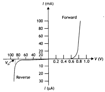
Draw V-l characteristics of a p-n junction diode. Answer the following questions, giving reasons:
(i) Why is the current under reverse bias almost independent of the applied potential up to a critical voltage?
(ii) Why does the reverse current show a sudden increase at the critical voltage? Name any semiconductor device which operates under the reverse bias in the breakdown region. (CBSEAI 2013)
Answer:
The characteristics are as shown.
(i) This is because even a small voltage is sufficient to sweep the minority carriers from one side of the junction to the other side of the junction.
(ii) As the reverse bias voltage is increased, the electric field at the junction becomes significant. When the reverse bias voltage V = Vz critical voltage, then the electric field strength is high enough to pull valence electrons from the host atoms on the p-side which are accelerated to the n-side. These electrons account for the high current observed at the breakdown.
Zener diode operates under the reverse bias in the breakdown region.
Question 4.
Draw the energy band diagrams of (i) n-type and (ii) p-type semiconductor at temperature T > 0 K.
In the case of n-type Si semiconductors, the donor energy level is slightly below the bottom of the conduction band, whereas in p-type semiconductors, the acceptor energy level is slightly above the top of the valence band. Explain what role do these energy levels play in conduction and valence bands. (CBSE AI 2015 C)
Answer:
For energy bands
(i) The energy level diagram is shown below.
(ii) The diagram is shown as
In the energy band diagram of n-type Si semiconductor, the donor energy level EA is slightly below the bottom Ec of the conduction band and electrons from this level move into the conduction band with a very small supply of energy. At room temperature, most of the donor atoms get ionized but very few (-10-12) atoms of Si get ionized. So the conduction band will have most electrons coming from the donor impurities.
Similarly, for p-type semiconductors, the acceptor energy level EA is slightly above the top Ev of the valence band. With the very small supply of energy, an electron from the valence band can jump to the level EA and ionize the acceptor negatively. Alternately, we can also say that with a very small supply of energy, the hole from level EA sinks down into the valence band. Electrons rise up and holes fall down when they gain external energy.
Question 5.
Give reasons for the following:
(i) High reverse voltage does not appear across an LED.
Answer:
It is because the reverse breakdown voltage of LED is very low, i.e. nearly 5 V.
(ii) Sunlight is not always required for the working of a solar cell.
Answer:
Because solar cells can work with any light whose photon energy is more than the bandgap energy.
(iii) The electric field, of the junction of a Zener diode, is very high even for a small reverse bias voltage of about 5 V. (CBSE Delhi 2016C)
Answer:
The heavy doping of p and n sides of the p-n junction makes the depletion region very thin, hence for a small reverse bias voltage, the electric field is very high.
Question 6.
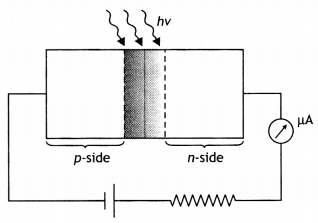
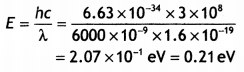
State the reason why the photodiode is always operated under reverse bias. Write the working principle of operation of a photodiode. The semiconducting material used to fabricate a photodiode has an energy gap of 1.2 eV. Using calculations, show whether it can detect light of a wavelength of 400 nm incident on it. (CBSE Al 2017C)
Answer:
It is easier to observe the change in the current with the change in the light intensity if a reverse bias is applied. Thus photodiode is used in the reverse bias mode even when the current in the forward bias is more the energy gap (Eg) of the semiconductor, then electron-hole pairs are generated due to the absorption of photons.
Due to the electric field of the junction, electrons and holes are separated before they recombine. The direction of the electric field is such that electrons reach the n-side and holes reach the p-side. Electrons are collected on the n-side and holes are collected on the p-side giving rise to an emf. When an external load is connected, current flows.
Given λ = 400 nm,
Energy of photon
E = \(\frac{h c}{\lambda}=\frac{6.63 \times 10^{-34} \times 3 \times 10^{8}}{400 \times 10^{-9} \times 1.6 \times 10^{-19}}\) = 3.105 eV
Since the bandgap is lesser than this energy, therefore it will be able to detect the wavelength.
Question 7.
Explain the two processes involved in the formation of a p-n junction diode. Hence define the term ‘barrier potential’. (CBSE Delhi 2017C)
Answer:
The two processes are
(i) Diffusion and
(ii) Drift
- Diffusion: The holes diffuse from the p-side to the n-side and electrons diffuse from the n-side to the p-side.
- Drift: The motion of charge carriers due to the applied electric field which results in the drifting of holes along the electric field and of electrons opposite to the electric field.
The potential barrier is the fictitious battery that seems to be connected across the junction with its positive end on the n-type and the negative end on the p-type.
Question 8.
Explain briefly how a photodiode operates.
Answer:
A Photodiode is again a special purpose p-n junction diode fabricated with a transparent window to allow light to fall on the diode. It is operated under reverse bias. When the photodiode is illuminated with light (photons) with energy (hv) greater than the energy gap (Eg) of the semiconductor, then electron-hole pairs are generated due to the absorption of photons. The diode is fabricated such that the generation of e-h pairs takes place in or near the depletion region of the diode.
Question 9.
Name the p-n junction diode which emits spontaneous radiation when forward biased. How do we choose the semiconductor, to be used in these diodes, if the emitted radiation is to be in the visible region?
Answer:
The p-n junction diode, which emits spontaneous radiation when forward biased, is the “light-emitting diode” or LED.
The visible tight is from 400 nm to 700 nm and the corresponding energy is between 2.8 eV to 1.8 eV. Therefore, the energy gap of the semiconductor to be used in LED, in order to have the emitted radiation be in the visible region, should be 1.8 eV. Phosphorous doped gallium arsenide and gallium phosphide are two such suitable semiconductors.
Question 10.
The figure shows the V-l characteristic of a semiconductor diode designed to operate under reverse bias. (CBSE Al 2019)
(a) Identify the semiconductor diode used.
Answer:
The diode used is Zener diode
(b) Draw the circuit diagram to obtain the given characteristics of this device.
Answer:
The circuit diagram is as shown.
(c) Briefly explain one use of this device.
Answer:
The Zener diode can be used as a voltage regulator in its breakdown region. The Zener voltage remains constant even when the current through the Zener diode changes.
Question 11.
With the help of a diagram, show the biasing of a light-emitting diode (LED). Give its two advantages over conventional incandescent lamps.
Answer:
The biasing of a light-emitting diode (LED), has been shown below.
Two main advantages of LED over conventional incandescent lamps are as follows:
- Low operational voltage and less power consumption.
- Fast action and no warm-up time required.
- The bandwidth of emitted light is 100 A to 500 A or in other words, it is nearly (but not exactly) monochromatic.
- Long life and ruggedness.
- Fast on-off switching capability.
Question 12.
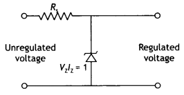
(a) Writetheprincipleofasemiconductor device which is used as a voltage regulator.
Answer:
(a) Zener diode is used as a voltage regulator
Principle: It is based on the Principle that when breakdown voltage V2 takes place, there is a large change in the reverse current even with the insignificant change in the reverse bias voltage.
(b) With the help of a circuit diagram explain its working.
Answer:
Working: If the reverse voltage across a Zener diode is increased beyond the breakdown voltage Vz, the current increases sharply and large current lz flows through the Zener diode and the voltage drop across Rs increases maintaining the voltage drop across RL at constant value Vo = Vz.
On the other hand, if we keep the input voltage constant and decrease the load resistance RL, the current across the load will increase. The extra current cannot come from the source because drop-in Rs will not change as the Zener is within its regulating range. The additional load current will pass through the Zener diode and is known as Zener current lz so that the total current (lL + lz) remains constant.
(c) Draw its l-V characteristics. (CBSE 2019C)
Answer:
l-V Characteristics of Zener diode
Question 13.
With what considerations in view, a photodiode is fabricated? State its working with the help of a suitable diagram.
Even though the current in the forward bias is known to be more than in the reverse bias, yet the photodiode works in reverse bias. What is the reason? (CBSE Delhi 2015)
Answer:
It is fabricated with a transparent window to allow light to fall on the diode. It is fabricated such that the generation of e-h pairs takes place in or near the depletion region of the diode.
When the photodiode is illuminated with light (photons) with energy (hw) greater than the energy gap (Eg) of the semiconductor, then electron-hole pairs are generated due to the absorption of photons. The diode is fabricated such that the generation of e-h pairs takes place in or near the depletion region of the diode. Due to the electric field of the junction, electrons and holes are separated before they recombine.
The direction of the electric field is such that electrons reach the n-side and holes reach the p-side. Electrons are collected on the n-side and holes are collected on the p-side giving rise to an emf. When an external load is connected, current flows. The magnitude of the photocurrent depends on the intensity of incident light (photocurrent is proportional to incident light intensity). The diagram is as shown.
It is easier to observe the change in the current with a change in the light intensity if a reverse bias is applied. Thus photodiode is used in the reverse bias mode even when the current in the forward bias is more.
Question 14.
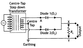
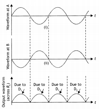
Draw the circuit diagram of a full-wave rectifier and explain its working. Also, give the input and output waveforms. (CBSE Delhi 2019)
Answer:
The circuit diagram is as shown.
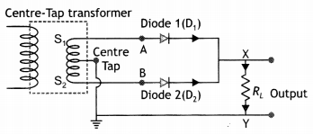
The two ends S1 and S2 of a center-tapped secondary of a transformer are connected to the P sections of the two diodes D1 and D2 respectively. The n-sections of the two diodes are joined together and their com¬mon junction is connected to the central tap C of the secondary winding through a load resistance RL. The input is applied across the primary and the output is ob¬tained across the load resistance RL. The arrows show the direction of the current.
Assume that the end A of the secondary is positive during the first half cycle of the supply voltage. This makes diode D1 forward biased and diode D2 reverse biased. Thus diode D1 conducts and an output is obtained across the load RL.
During the second half cycle of the supply voltage, the polarities of the secondary windings reverse. A becomes negative and B becomes positive with respect to the central terminal C. This makes diode D2 forward biased. Hence it conducts and an output is obtained across RL.
The input-output waveforms are as shown.
Question 14.
Draw the circuit diagram to show the use of a p-n junction diode as a half-wave rectifier. Also show the input and the output voltages, graphically. Explain its working.
Answer:
The diagram is as shown.
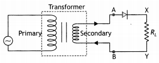
The input and output waveforms are as shown.
A p-n junction diode is used as a half-wave rectifier. Its work is based on the fact that the resistance of the p-n junction becomes low when forward biased and becomes high when reversing biased. These characteristics of a diode are used in rectification.
Question 15.
Distinguish between conductors, insulators, and semiconductors on the basis of the band theory of solids.
Answer:
The diagrams are as shown.
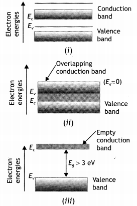
Metals: A distinguishing character of all conductors, including metals, is that the valence band is partially filled or the conduction and the valence band overlap. Electrons in states near the top of the filled portion of the band have many adjacent unoccupied states available, and they can easily gain or lose small amounts of energy in response to an applied electric field. Therefore these electrons are mobile and can contribute to electrical and thermal conductivity. Metallic crystals always have partially filled bands figure (ii).
Insulators: In the case of insulators, there is a large energy gap of approximately 6 eV depending upon the nature of the crystal. Electrons, however, heated, find it difficult or practically impossible to jump this gap and thus never reach the conduction band. Thus electrical conduction is not possible through an insulator figure (iii).
Semiconductors: There is a separation between the valence band and the conduction band. The energy gap is of the order of 1 eV (0.67 eV for germanium and 1.12 eV for silicon). At absolute zero the electrons cannot gain this energy. But at room temperature, these electrons gain energy and move into the conduction band where they are free to move even under the effect of a weak electric field figure (i).
Question 16.
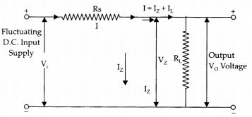
What is a Zener diode? How is it symbolically represented? With the help of a circuit diagram, explain the use of the Zener diode as a voltage stabilizer.
Answer:
It is a special diode made to work only in the reverse breakdown region.
Symbol:
The figure below shows the use of the Zener diode in providing a constant voltage supply.
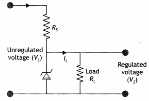
This use of the Zener diode is based on the fact that in the reverse breakdown (or Zener) region, a very small change in voltage across the Zener diode produces a very large change in the current through the circuit. If voltage is increased beyond Zener voltage, the resistance of the Zener diode drops considerably. Consider that the Zener diode and a resistor R, called dropping resistor, are connected to a fluctuating voltage supply, such that the Zener diode is reverse biased.
Whenever voltage across the diode tends to increase, the current through the diode rises out of proportion and causes a sufficient increase in the voltage drop across the dropping resistor. As a result, the output voltage lowers back to the normal value. Similarly, when the voltage across the diode tends to decrease, the current through the diode goes down out of proportion, so that the voltage drop across the dropping resistor is much less and now the output voltage is raised to normal.
Question 17.
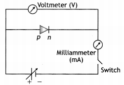
Explain briefly with the help of a circuit diagram how V-l characteristics of a p-n junction diode are obtained in (i) forward bias and (ii) reverse bias.
Answer:
Forward biased characteristics: A p-n junction is said to be forward-biased if its p-type is connected to the positive terminal and its n-type is connected to the negative terminal of a battery shows a circuit diagram that is used to study the forward characteristics of a p-n junction. The p-n junction is forward biased. Different readings are taken by changing the voltage and noting the corresponding milliammeter current.
Practically no current is obtained till the applied voltage becomes greater than the barrier potential. Above the potential barrier voltage, even a small change in potential causes a large change in current.
Reverse biased characteristics: In reverse biased characteristics, instead of a milliammeter, a microammeter is used. The voltage across the p-n junction is increased and the corresponding current is noted.
In the reverse bias, the diode current is very small. As the voltage has increased the current also increases. At a certain voltage, the current at once becomes very large. This voltage is called Breakdown voltage or Zener voltage. At this voltage, a large number of covalent bonds break releasing a large number of electrons and holes. Hence a large current is obtained. The characteristics are as shown.
Question 18.
Explain how the heavy doping of the p and n sides of a p-n junction diode helps in internal field emission (or Zener breakdown), even with a reverse bias voltage of a few volts only. Draw the general shape of the V-I characteristics of a Zener diode. Discuss how the nature of these characteristics led to the use of a Zener diode as a voltage regulator.
Answer:
Consider a p-n junction where both p- and n-sides are heavily doped. Due to the high dopant densities, the depletion layer junction width is small and the junction field will be high. Under large reverse bias, the energy bands near the junction and the junction width decrease. Since the junction width is < 10-7 m, even a small voltage (say 4 V) may give a field as large as 4 × 10⁻⁷ Vm-1. The high junction field may strip an electron from the valence band which can tunnel to the n-side through the thin depletion layer. Such a mechanism of emission of electrons after a certain critical field or applied voltage V is termed as internal field emission which gives rise to a high reverse, current, or breakdown current.
The general shape of the V-l characteristics of a Zener diode is as shown in the figure.
Suppose an unregulated dc input voltage (Vi) is applied to the Zener diode (whose breakdown voltage is Vz as shown in the figure. If the applied voltage Vi > Vz, then the Zener diode is in the breakdown condition. As a result of a wide range of values of load (RL), the current in the circuit or through the Zener diode may change but the voltage across it remains unaffected by the load. Thus, the output voltage across the Zener is a regulated voltage.
Question 19.
(i) Describe briefly with the help of a necessary circuit diagram, the working principle of a solar cell.
Answer:
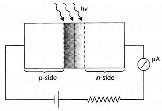
Solar Cell: A solar cell is a junction diode that converts solar energy into electrical energy. In a solar cell, the n-region is very thin and transparent so that most of the incident light reaches the junction. The thin region is called the emitter and the other base. When light is incident on it, it passes through the crystal onto the junction. The electrons and holes are generated due to light (with hv > Eg). The electrons are kicked to the n-side and holes to the p-side due to the electric field of the depletion region. Thus p-side becomes positive and the n-side becomes negative giving rise to a photo-voltage. Thus it behaves as a cell.
(ii) Why are Si and GaAs preferred materials for solar cells? Explain. (CBSE AI 2011C)
Answer:
Si and GaAs are preferred for solar cell fabrication due to the fact that their bandgap is ideal. Further, they have high electrical conductivity and high optical absorption.
Question 20.
Explain, with the help of a circuit diagram, the working of a photo-diode. Write briefly how it is used to detect optical signals. (CBSE Delhi 2013)
Answer:
When the photodiode is illuminated with light (photons) with energy (hv) greater than the energy gap (Eg) of the semiconductor, then – electron-hole pairs are generated due to the absorption of photons. The diode is fabricated such that the generation of e-h pairs takes place in or near the depletion region of the diode. Due to the electric field of the junction, electrons and holes are separated before they recombine. The direction of the electric field is such that electrons reach the n-side and holes reach the p-side. Electrons are collected on the n-side and holes are collected on the p-side giving rise to an emf. When an external load is connected, current flows.
The magnitude of the photocurrent depends on the intensity of incident light incident on it. This helps in detecting optical signals.
Question 21.
(i) Explain with the help of a diagram, how depletion region and potential barrier are formed in a junction diode.
(ii) If a small voltage is applied to a p-n junction diode, how will the barrier potential be affected when it is (i) forward biased and (ii) reverse biased? (CBSE AI2015)
Answer:
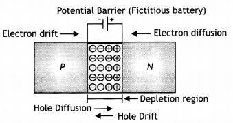
(i) Since there is an excess of electrons in the n-type and excess of holes in the p-type, on the formation of a p-n junction the electrons from the n-type diffuse into the p-region, and the holes in the p-type diffuse into the n-region.
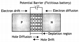
The accumulation of electric charge of opposite polarities in the two regions across the junction establishes a potential difference between the two regions. This is called the potential barrier or junction barrier. The potential barrier developed across the junction opposes the further diffusion of the charge carriers from p to n and vice versa. There is a region on either side of the junction where there is a depletion of mobile charges and has only immobile charges. The region around the junction, which is devoid of any mobile charge carriers, is called the depletion layer or region.
(ii) (a) In forwarding bias the potential barrier decreases.
(b) In reverse bias the potential barrier increases.
Question 22.
Write the two processes that take place in the formation of a p-n junction. Explain with the help of a diagram, the formation of depletion region and barrier potential in a p-n junction. (CBSE Delhi 2017)
Answer:
- Drift and
- diffusion.
The n-type has an excess of electrons and the p-type has an excess of holes. When a p-n junction has formed the electrons from the n-type diffuse into the p-region and the holes in the p-type diffuse into the n-region. These diffusing electrons and holes combine near the junction. Each combination eliminates an electron and a hole. This results in the n-region near the junction becoming positively charged by losing its electrons and the p-region near the junction becoming negatively charged by losing its holes.
This accumulation of electric charge of opposite polarities in the two regions across the junction establishes a potential difference between the two regions. This is called the potential barrier or junction barrier.
The potential barrier developed across the junction opposes the further diffusion of the charge carriers from p to n and vice versa. As a result, a region develops on either side of the junction where there is a depletion of mobile charges and has only immobile charges. The region around the junction which is devoid of any mobile charge carriers is called the depletion layer or region.
Question 23.
(i) State briefly the processes involved in the formation of the p-n junction explaining clearly how the depletion region is formed.
Answer:
As we know that n-type semi-conductor has more concentration of electrons than that of a hole and a p-type semi-conductor has more concentration of holes than an electron. Due to the difference in concentration of charge carriers in the two regions of the p-n junction, the holes diffuse from p-side to n-side, and electrons diffuse from n-side to p-side. When an electron diffuses from n to p, it leaves behind it an ionized donor on the n-side. The ionized donor (+ve charge) is immobile as it is bound by the surrounding atoms. Therefore, a layer of positive charge is developed on the n-side of the junction. Similarly, a layer of negative charge is developed on the p-side.
Hence, a space-charge region is formed on either side of the junction, which has immobile ions and is devoid of any charge carrier, called depletion layer or depletion region.
The potential barrier is the fictitious battery which seems to be connected across the junction with its positive end on the n-type and the negative end on the p-type.
(ii) Using the necessary circuit diagrams, show how the V – l characteristics of a p-n junction are obtained in
(a) Forward biasing
(b) Reverse biasing
How these characteristics are made use of in rectification? (CBSE Delhi 2014)
Answer:
(a) p-n junction diode under forwarding bias: The p-side is connected to the positive terminal and the n-side to the negative terminal. Applied voltage drops across the depletion region. Electron in n-region moves towards the p-n junction and holes in the p-region move towards the junction. The width of the depletion layer decreases and hence, it offers less resistance. Diffusion of majority carriers takes place across the junction. This leads to the forward current.
(b) p-n junction diode under reverse bias: Positive terminal of the battery is connected to the n-side and negative terminal to p-side. Reverse bias supports the potential barrier. Therefore, the barrier height increases and the width of the depletion region also increases. Due to the majority of carriers, there is no conduction across the junction. A few minority carriers across the junction after being accelerated by the high reverse bias voltage. This constitutes a current that flows in opposite direction, which is called reverse current.
For V-l curves
A p-n junction diode is used as a half-wave rectifier. Its work is based on the fact that the resistance of the p-n junction becomes low when forward biased and becomes high when reversing biased. These characteristics of the diode are used in rectification.
Question 24.
(i) Explain with the help of a suitable diagram, the two processes which occur during the formations of a p-n junction diode. Hence define the terms (i) depletion region and (ii) potential barrier.
(ii) Draw a circuit diagram of a p-n junction diode under forwarding bias ‘ and explain its working. (CBSE 2018C)
Answer:
(i) The two important processes are diffusion and drift.
Due to the concentration gradient, the electrons diffuse from the n-side to the p side, and holes diffuse from the n-side to the n side.
Due to the diffusion, an electric field develops across the junction. Due to the field, an electron moves from the p-side to the n-side; a hole moves from the n-side to the p-side. The flow of the charge carriers due to the electric field is called drift.
(a) Depletion region: It is the space charge region on either side of the junction that gets depleted of free charges is known as the depletion region.
(b) Potential Barrier: The potential difference that gets developed across the junction and opposes the diffusion of charge carriers and brings about a condition of equilibrium, which is known as the barrier potential.
(ii) The circuit diagram is as shown
Working:
In the forward bias condition, the direction of the applied voltage is opposite to the barrier potential. This reduces the width of the depletion layer as well as the height of the barrier. A current can, therefore, flow through the circuit. This current increases (non¬linearly) with the increase in the applied voltage.
Numerical Problems
Question 1.
(i) Three photodiodes D1, D2, and D3 are made of semiconductors having band gaps of 2.5 eV, 2 eV, and 3 eV respectively. Which of them will not be able to detect light of wavelength 600 nm? (CBSE Delhi 2019)
Answer:
λ = 600 nm
The energy of a photon of wavelength λ
E = \(\frac{h c}{\lambda}=\frac{6.63 \times 10^{-34} \times 3 \times 10^{8}}{600 \times 10^{-9} \times 1.6 \times 10^{-19}}\) = 2.08 eV
The bandgap energy of diode D2 (= 2eV) is less than the energy of the photon. Hence diode D2 will not be able to detect light of wavelength 600 nm.
(ii) Why photodiodes are required to operate in reverse bias? Explain.
Answer:
A photodiode when operated in reverse bias can measure the fractional change in minority carrier dominated reverse bias current with greater ease than when forward biased.
Question 2.
In half-wave rectification, what is the output frequency if the input frequency is 50 Hz? What is the output frequency of a full-wave rectifier for the same input frequency? (NCERT)
Answer:
The output frequency of the half-wave rectifier is the same as the input frequency, while that of the full-wave rectifier is double that of the input. Therefore the frequency is 50 Hz for half-wave and 100 Hz for full-wave.
Question 3.
A p-n photodiode is fabricated from a semiconductor with a bandgap of 2.8 eV. Can it detect a wavelength of 6000 nm? (NCERT)
Answer:
Given λ = 6000 nm,
Energy of photon
Since the bandwidth is greater than this energy, it will not be able to detect the wavelength.
Question 4.
Three photodiodes D1, D2, and D3 are made of semiconductors having band gaps of 2.5 eV, 2 eV, and 3 eV, respectively. Which ones will be able to detect light of wavelength 600 nm? (NCERT Exemplar)
Answer:
The energy of an incident light photon is given by
For the incident radiation to be detected by the photodiode, the energy of the incident radiation photon should be greater than the bandgap. This is true only for D2. Therefore, only D2 will detect this radiation.
Question 5.
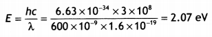
If each diode in the figure has a forward bias resistance of 25 Ω and infinite resistance in reverse bias, what will be the values of the current l1 l2, l3, and l4? (NCERT Exemplar)
nswer:
Current l3 is zero as the diode in that branch is reverse biased.
Resistance in the branches AB and EF is each (125 +25) Ω = 150 Ω
As AB and EF are identical paraLleL branches, their effective resistance is 150/2 = 75 Ω
Therefore net resistance in the circuit Is
Rnet =75 + 25 = 100 Ω
Therefore current l1 is
l1 = 5/100 = o.05 A
As resistance of branches AB and EF is equal, the current l1 will be equally shared by the two, hence
l2 = l4 = 0.05/2 = 0.025A
Hence l1 = 0.05 A, l2 = l4 = 0.025 A, l3 = 0
Question 6.
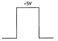
Assuming the ideal diode, draw the output waveform for the circuit given in the figure. ExplaIn the waveform. (NCERT Exemplar)
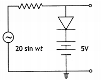
Answer:
When input voltage Will is greater than 5 V, the diode wilt becomes forward biased and will conduct. When the input is Less than 5 V, the diode will be reverse biased and will not conduct, i.e. open circuit, hence the output is as shown.